Contact Press / Media
Petra Nolis M.A.
Group leader Communications
Fraunhofer Institute for Laser Technology ILT
Steinbachstr. 15
52074 Aachen
Phone +49 241 8906-662
Fax +49 241 8906-121
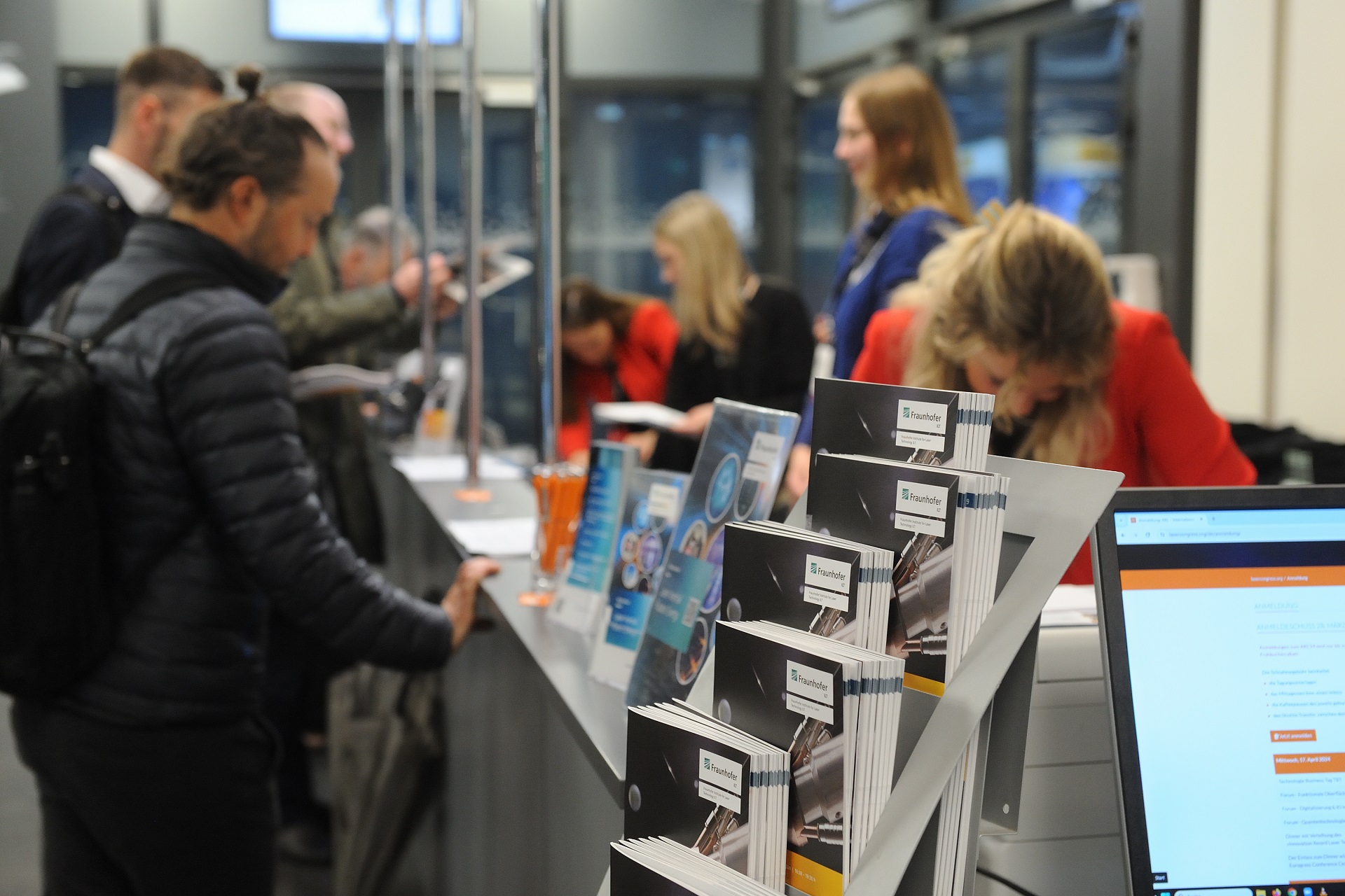
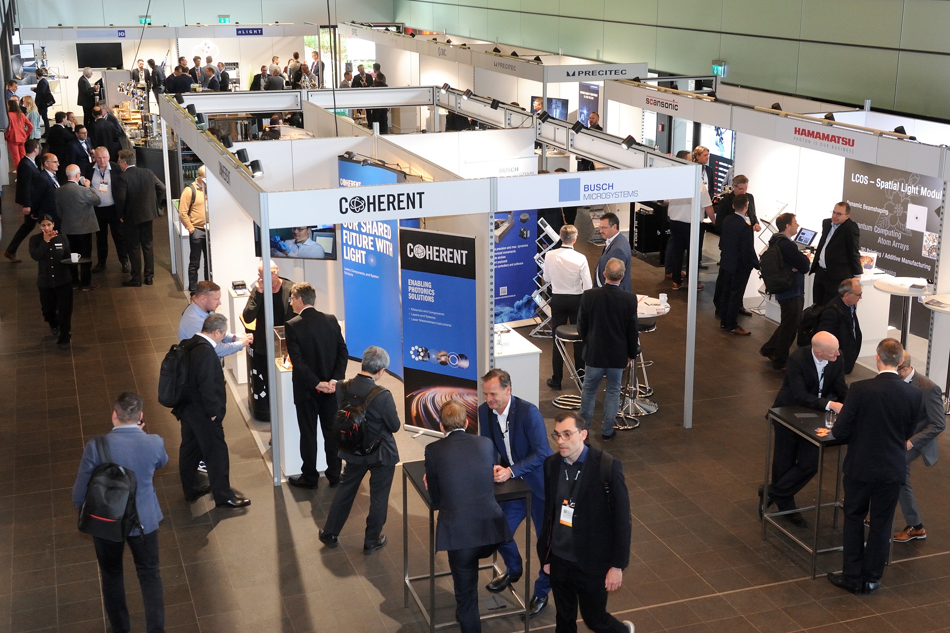
The “AKL’24 - International Laser Technology Congress” took place in Aachen from April 17 to 19, 2024. For the 14th time, the congress provided a platform for an intensive professional exchange on current technology trends and perspectives in laser technology. In addition to three forums and nine sessions with a total of 82 specialist presentations, the 525 participants from 21 countries had access to a fully booked exhibition with 58 companies and 60 “Laser Technology Live” demonstrations in the laboratories of the Fraunhofer Institute for Laser Technology ILT and RWTH Aachen University. Two evening events and the deliberately relaxed schedule on the three days of the congress invited participants to network. In short: AKL’24 was the place to be for the laser community.
The forums and sessions of the three-day congress will inevitably take place in parallel, especially as the interests and focal points of the participants differ. At the same time, the AKL stands for professional depth. It bridges the gap between application-oriented research and practical applications. Technology suppliers and customers meet here, develop questions, goals and visions together, and use the congress to bring each other up to date.
This transfer is taking place in various specialist domains. Lasers are fulfilling an increasingly broad spectrum of tasks in surface technology, additive manufacturing and medical technology; they cut and join metals and plastics, generate three-dimensional microstructures inside glass and can be used to produce semiconductor and electronics on a micrometer scale. Nevertheless, in the six decades since the laser was invented, the laser industry has only tapped a fraction of its actual technological and economic potential. “The laser has not been fully explored. On the contrary- 60 years after its invention, it is only just getting started!” said Prof. Constantin Haefner, Director of the Fraunhofer ILT in Aachen, in his closing speech at AKL’24.
New beam sources, improved optical systems and optimized processes are needed to exploit the full potential. While the first laser applications literally resembled a rough hand axe, quantum technologies today operate on the scale of individual photons, ions and atoms. Surface technology and optical coatings achieve similar precision. And when the world's largest laser system at the National Ignition Facility of the Lawrence Livermore National Laboratory in California directs its concentrated pulsed energy at a pinhead-sized pellet containing the hydrogen isotopes deuterium and tritium, igniting their fusion, it releases the same amount of energy as burning eleven tons of coal. At the same time, inertial confinement fusion is climate-neutral and intrinsically safe.
In its three forums and nine sessions, AKL’24 got to the bottom of all the topics it covered – surface technology, cutting and joining, additive manufacturing and process optimization with the help of digitalization and artificial intelligence, optical systems and new beam sources, as well as future-oriented laser applications in medical technology, quantum technologies and nuclear fusion. Every look back on this congress is also a look into the future of photonics.
The leitmotif of AKL’24 was one question: How can photonics harness the potential of artificial intelligence (AI) as quickly as possible?
Since process chains are becoming increasingly digitalized, more and more networked machines and sensors are generating an enormous amount of data. This applies to research, development and design as well as to photonic production and product life cycles. AI and machine learning are opening up new opportunities to refine the abundant raw material of data. “Just as the value of crude oil only becomes apparent when it is broken down into its components and further processed into fuels, plastics and chemicals, it is important to break down data, analyze it and derive information with added value from it,” said Michael Lebrecht right at the start of AKL’24 at the “Digitalization and AI in Photonic Production” forum. The manager for Industrial Robotics and Manufacturing Processes at Mercedes-Benz AG thus set the tone that was echoed in many of the presentations throughout the congress.
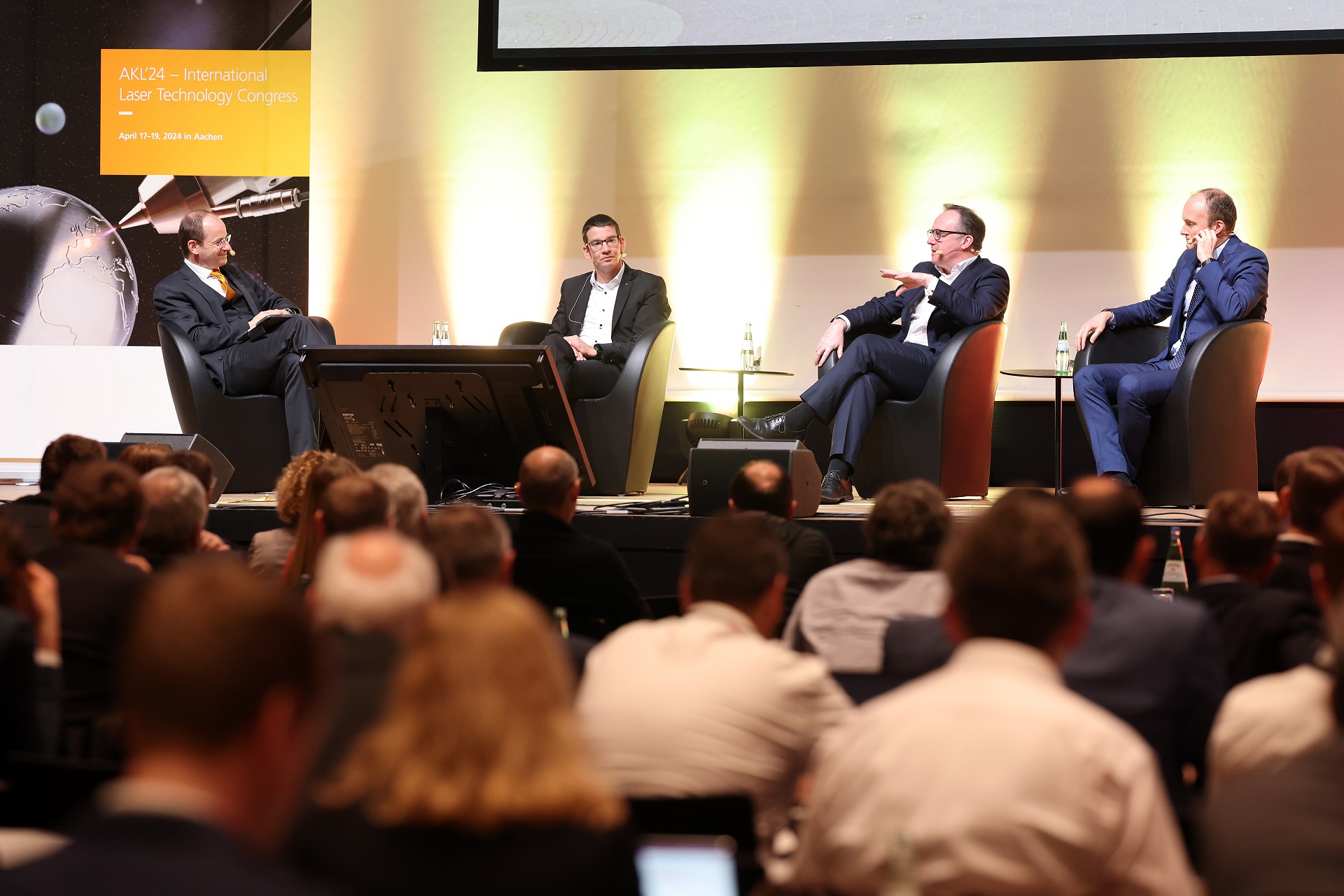
AI is becoming a tool for data-based photonic production. The question now is how quickly suppliers of laser systems, sensors and optics can tap into its technological and economic potential. “Access to data and the ability to derive added value from it with the help of AI are already synonymous with competitive advantages,” stated Prof. Constantin Haefner, Director of the Fraunhofer Institute for Laser Technology ILT in Aachen. In the “Gerd Herziger Session,” he discussed what this means for value creation and business models with top managers from the industry: Dr. Hagen Zimer, Member of the Management Board and CEO Laser Technology at TRUMPF SE + Co KG, Dr. Christopher Dorman, Executive Vice President of the COHERENT Lasers Business and Dr. Christoph Rüttimann, CTO of the Bystronic Group.
Like Fraunhofer ILT, the three companies are working intensively with AI and are driving forward the digital networking of their processes, products and organizations; if necessary, they call in external expertise. The tenor of the discussion: AI replicates the evolutionarily perfected neuronal learning processes of the human brain at the speed of light and filters information from very heterogeneous data that was previously inaccessible. Correspondingly trained algorithms scan sensor and camera data systematically and, if necessary, in real time for deviations and errors that typically occur in laser machining processes. In their presentations, Dr. Markus Kogel-Hollacher from Precitec Optronic GmbH and Dr. Michael Ungers from Scansonic MI GmbH demonstrated how their companies use these possibilities to monitor in real-time, to document seamlessly and to optimize laser welding and laser soldering processes.
The presentations made it clear that the combination of AI methods with different measurement and sensor technology – including cameras, pyrometers or photodiodes for recording process emissions as well as OCT (Optical Coherence Tomography) and laser-acoustic sensors – offers possibilities that go far beyond conventional detection and documentation of defects and deviations. AI-supported analysis methods can also be used to determine what causes defects and deviations if the generated measurement and sensor signals are synchronized with process and system data – for example, the performance data of the lasers – using time stamps. This would be the first step towards readjusting parameters in ongoing laser processes so that quality defects do not occur in the first place or can at least be detected immediately: Photonic production processes would thus come very close to the goal of zero defect manufacturing (ZDM). The “Digitalization and AI in Photonic Production” forum has shown that this vision is certainly within the realms of possibility: Suppliers of sensor technology and laser processes are working intensively with AI and systematically towards the “AI readiness” of their products and processes that Zimer, Rüttimann and Dorman called for at the “Gerd Herziger Session.”
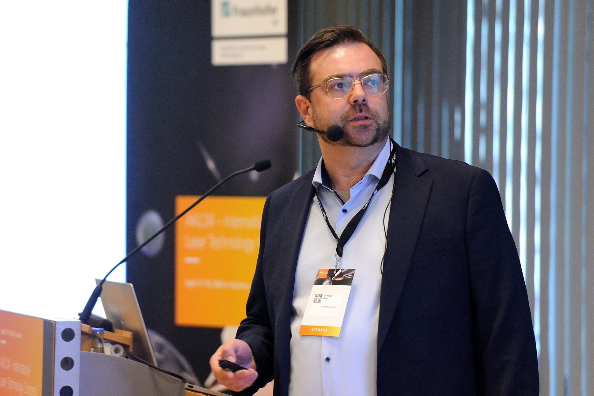
Christoph Franz, the managing partner of 4D Photonics GmbH, presented an approach for implementing multi-sensor technology with a single sensor. Despite its small edge length of 91 x 63 x 79 mm, it detects a wide range of wavelengths on 32 channels with a sampling rate of six kilohertz each, and detects deviations of around 40 micrometers even at feed rates of 1,000 millimeters per second. Since the channels can be combined as required, the sensor also records acoustic emissions, humidity, air pressure and temperature. Moreover, since it can be connected to any third-party sensor system, the tiny device generates an enormous database: It delivers around one million samples per second.
With AI, errors and their causes can be identified during the ongoing process because the signals are based on defined physical measured variables. 4D Photonics uses preliminary analyses to determine which spectral ranges best reveal relevant quality fluctuations for the respective applications and, thus, combines the most suitable channels. The evaluation is AI-based. Franz provided insights into test series at the Deutsches Elektronen Synchrotron DESY, in which the company was involved. The team used its sensor technology to monitor ongoing laser processes in parallel with a high-speed X-ray camera. “We can use the image data to precisely track when and where pores and other defects form in the weld pool of a weld seam, for example,” he explained. On this basis, they can understand exactly how these events are reflected in the 4D sensor signals. Currently, the institute is systematically evaluating over 100 terabytes of data from the four-week test series.
Its aim is to create the data basis for initial training of the AI. After this training, it should be able to independently identify defects and defect classes in industrial processes in the signals from the multispectral 4D sensors. Franz wants to gradually transfer what is currently starting with laser welding processes to other laser applications. However, the forum showed that there are hardly any application limits to such multisensory process monitoring: Be it for welding hairpins for electric motors, bipolar plates for fuel cells and battery housings for electric vehicles, for meticulous quality assurance in the coating of brake discs using extreme high-speed laser cladding (EHLA) or for optimizing laser cutting processes in fully automated systems. AKL’24 impressively demonstrated the potential of digitalization and, in particular, the use of AI and machine learning in photonic production – and that the photonics industry has long been working on leveraging this potential.
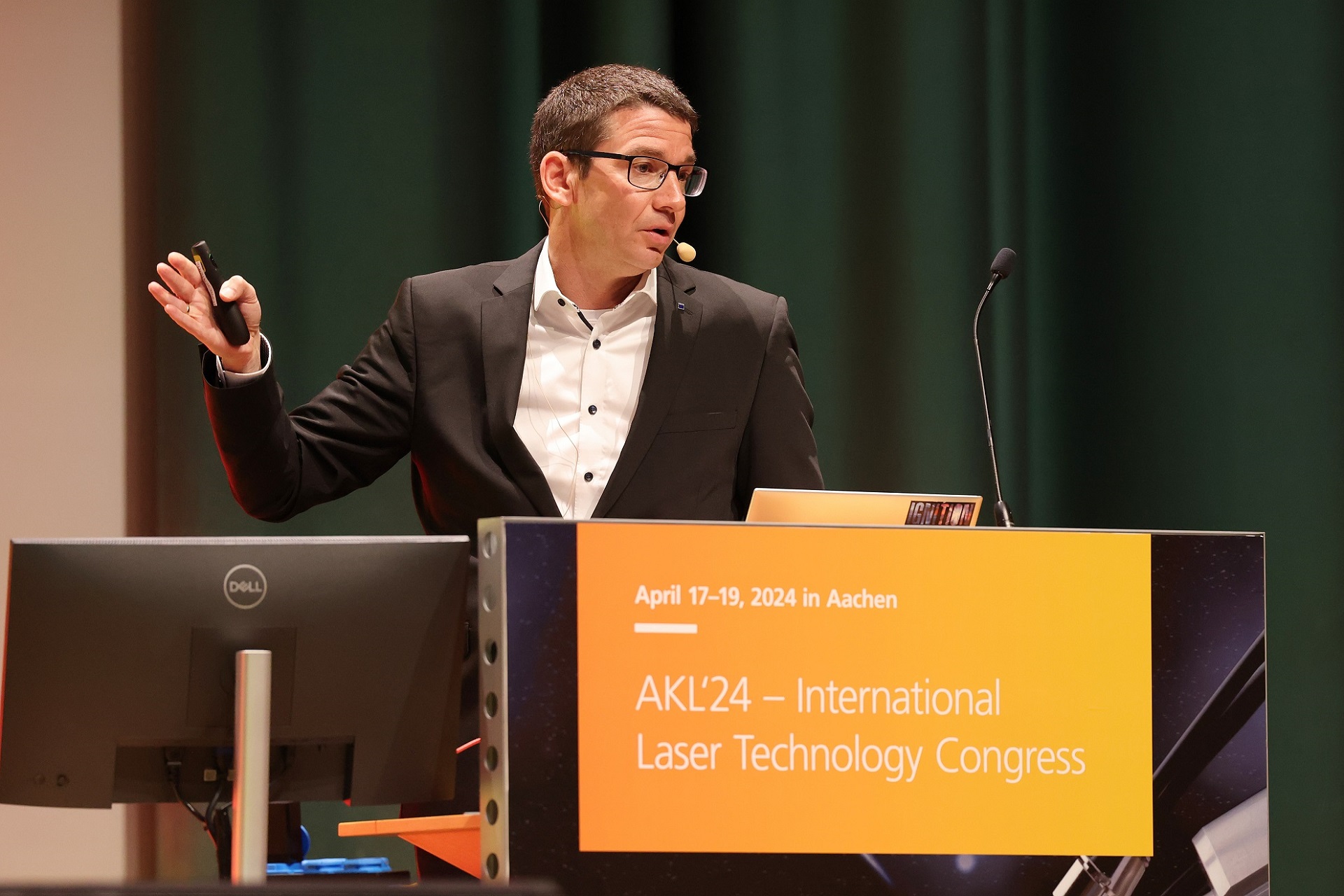
Whether in soft tissue surgery or for the ablation of hard tissue, lasers are becoming more and more important as a non-contact tool in the operating theater as they increasingly can play out their advantages over conventional surgical procedures in medical clinics. The “Medical Technology” session on the second conference day of the AKL - International Laser Technology Congress 2024 in Aachen provided insight into where laser procedures are already being used successfully in clinical practice. These include various areas of tumor surgery and ophthalmology, but laser technology can also improve therapies in neurosurgery in the future through precise and gentle interventions.
In neurosurgical procedures, certain indications require complex brain functions such as speech or motor function to be monitored during the operation: for example, awake deep brain stimulation operations for essential movement disorders such as tremor, Parkinson’s disease or dystonia. Such procedures are performed on locally anaesthetized, but awake patients. When removing certain brain tumors, surgeons operate on fully conscious patients in order to test complex brain functions and ensure that they are not impaired during the operation. To remove such tumor, doctors need to cut out a piece of the skull about the size of the palm of a hand. Until now, drills, saws and milling machines have been used for this purpose. The resulting vibrations and the noise transmitted through the skull bone are often traumatic for the psyche of those being treated. There is also a 10 percent risk of damaging the meninges or even the brain tissue when opening the skull.
PD Dr. Peter Reinacher from Freiburg University Hospital and the research team led by Dr. Achim Lenenbach from Fraunhofer ILT in Aachen are pursuing a new approach to awake surgery: together they are driving forward a laser procedure for stereotactic laser craniotomy that allows the skullcap to be opened gently, safely and almost silently. The Aachen team has developed a laser applicator that combines a high-energy laser beam with an interferometric measuring beam. The measuring beam uses optical coherence tomography (OCT) to measure the residual thickness of the skull bone during the removal of hard tissue with the cutting laser, a pulsed CO2 laser with a maximum pulse duration of 120 ns. This cuts the skull bone gently without noticeable vibration and without traumatizing drilling and milling noise. The residual thickness measurement of the skull bone regulates the cutting process and thus prevents damage to the meninges or brain under the skull.
In addition to developing the procedure for laser craniotomy, the team worked closely with neurosurgeons to connect the applicator to an existing stereotactic system and combine all components into a complete system. Thanks to its small footprint, its compatibility with the operating tables used and its sterility concept, it can be integrated into the workflow of an operating theater.
The procedure for laser-based bone ablation, which is being funded as part of the Fraunhofer research program ATTRACT under the project name STELLA, can also be used in other surgical disciplines where bone material has to be removed safely and precisely. In contrast to mechanical ablation processes, hard tissue ablation with laser radiation offers clear advantages in terms of safety, precision, minimal invasiveness and, last but not least, patient comfort during awake operations. The laser process is still being optimized on animal specimens before the next validation phase can be initiated.
In contrast, lasers have long been established in ophthalmology for both diagnostic and therapeutic applications. The most commonly used laser-based procedure to correct defective vision is LASIK (Laser Assisted in Situ Keratomeleusis). In this procedure, the top layer of the cornea is surgically opened and folded over so that the underlying cornea to be corrected can be processed with the laser. At AKL’24, Dr. Gregor Stobrawa from Carl Zeiss Meditec AG in Jena presented a new minimally invasive laser procedure for correcting myopia and astigmatism without external visual aids. The special feature of the so-called SMILE procedure is that a femtosecond laser beam at a wavelength of approx. 1 µm and pulse energies between 50 and 300 nJ penetrates the uppermost layer of the cornea without damaging it and ablates it in a circular fashion by focusing on the underlying corneal layers. The minimally invasive laser incision creates a tiny opening in the uppermost layer of the cornea through which the ablated tissue can then be removed. The altered curvature of the cornea corrects the refractive power of the eye and thus the defective vision. The procedure is much gentler on patients than previous laser procedures.
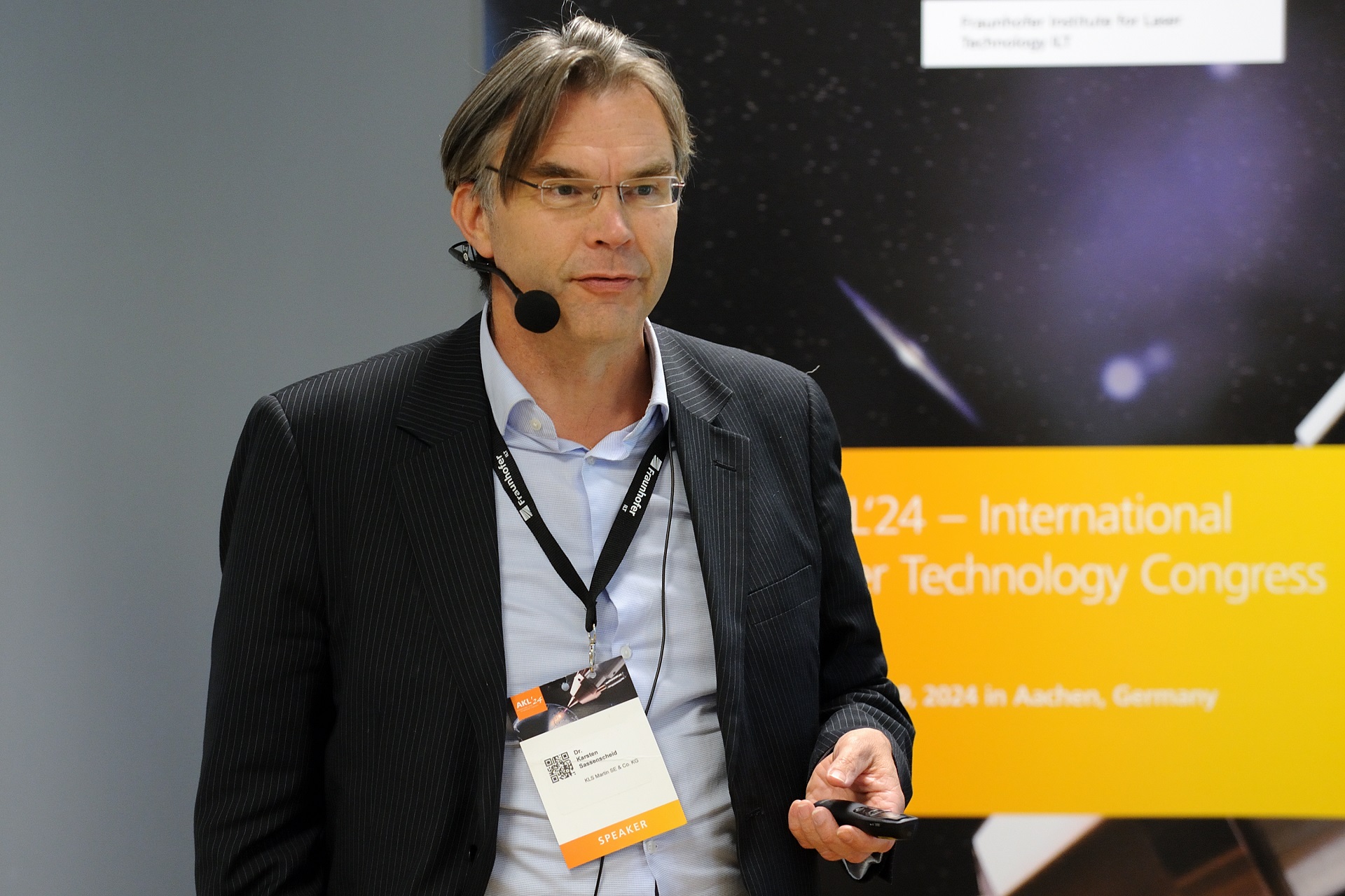
Dr. Karsten Sassenscheid from KLS Martin SE & Co. KG in Freiburg im Breisgau presented a minimally invasive laser procedure for tumour surgery. The surgeons use a diode-pumped Nd:YAG laser at a wavelength of 1320 nm to remove lung metastases. Both benign and malignant tumors on the vocal cords are also removed endoscopically using a so-called laryngoscope with the laser. CO2 lasers at a wavelength of 10,600 nm are used to cut the soft tissue. In both cases, special endoscopes allow minimally invasive access to the tumor, making it visible so that it can be removed precisely and gently with the laser.
Lasers have long been an established tool for surface processing. AKL’24 addressed this field of technology in the forum “Functional surfaces through laser processing” and in the session “Surface technology”; in both, the congress provided in-depth insight into a variety of innovative industrial applications. The spectrum ranged from functionalization for improving tribological properties, the production of high-temperature superconductors for use in microelectronics, space technology and renewable energies, to the production of self-cleaning and anti-reflective surfaces using direct laser interference patterning (DLIP) and the drying of battery electrodes with highly efficient diode lasers.
The latter was addressed by Dr. Simon Britten from Laserline GmbH in Mülheim-Kärlich in his presentation “Laser systems for the energy-efficient drying of battery electrodes.” Drying the anodes and cathodes coated with active material is time-consuming, requires a lot of space due to drying ovens that are almost 100 meters long, and accounts for almost 30 percent of the energy required for battery cell production. Efficient, powerful diode lasers can play out their advantages here: If they replace conventional processes, drying becomes 20 to 30 percent cheaper, the space required, and the drying time are reduced by almost two thirds – while consuming around 30 percent less energy. “Many other drying processes can also be carried out using lasers,” explained the expert.
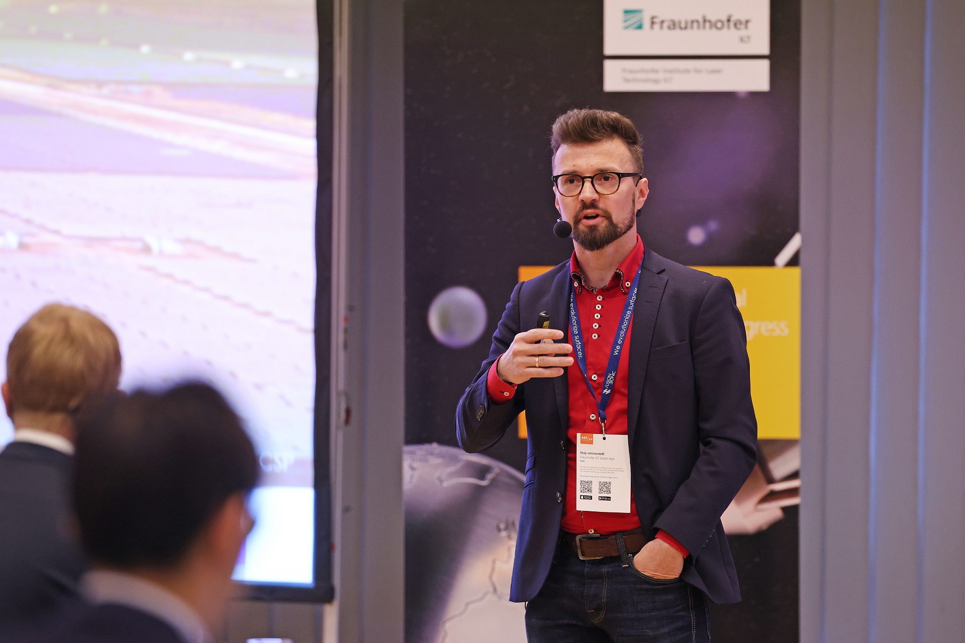
Dr. Tim Kunze, CEO of Fusion Bionic from Dresden, presented a process to precisely modify surfaces using direct laser interference patterning (DLIP). In this process, several laser beams are superimposed to generate functional surfaces, from anti-reflective coatings and non-slip tiles to self-cleaning surfaces. In many applications, the optical process can replace the use of aggressive chemicals and complex mechanical processing or expensive coatings. According to Kunze, the treatment of photovoltaic modules in particular holds great potential, because if they become dirty, the energy yield drops significantly. Consistent surface modification using DLIP could increase the solar power yield worldwide by 4 to 7th percent and reduce CO2 emissions by more than 18 million tons. In addition, solar park operators would be relieved of the burden of cleaning the modules, the water consumption of which generates high costs, especially in dry, dusty regions.
Other applications were presented by ASMPT Laser Separation International (ALSI) from Beuningen, Netherlands, and 3D-Micromac from Chemnitz, Germany. The latter presented an application in semiconductor production: so-called laser-assisted ohmic contact formation (OCF) based on laser annealing. This treatment reduces energy losses in switching regulators and increases performance and reliability both at voltages above 700 volts and in high-frequency and high-temperature processes. ASMPT also uses UV ultrashort pulse lasers in semiconductor production to prepare wafers for dicing, i.e. separating chips by means of a two-stage material ablation process. During this laser grooving, the picosecond-pulsed UV laser draws tiny boundaries along the active chip zones on both sides. This “trenching” is followed by the actual grooving, i.e. the removal of material at high power, in preparation for chip separation. In his presentation, Kees Biesheuvel used microscopic images to impressively demonstrate how precisely the UV-USP laser process performs this task in comparison to longer pulsed lasers in the green or infrared wavelength range, and at the same time improves the properties of the material.
In this presentation “Laser material processing in the field of electronic consumer goods,” Dr. Stefan Janssen from LG Electronics in South Korea demonstrated how laser technologies significantly improve the quality and efficiency of production processes for microelectronic devices and displays. The team of 60 researchers at LG Electronics' Production Research Institute (PRI) has 20 laser systems at its disposal. The high-performance systems reach processing speeds of up to 4,600 holes per second, with a positioning accuracy of 3 µm and hole diameters of less than 20 µm. According to Janssen, cutting speeds of more than 500 mm/s and a chipping size of less than 20 µm are feasible for high-speed cutting of ultra-thin glass (UTG). These advances in material processing not only improve product performance, but also lead to more reliable electronic devices, says Janssen. This is particularly important in a market in which consumers need to be convinced by high-quality, durable products.
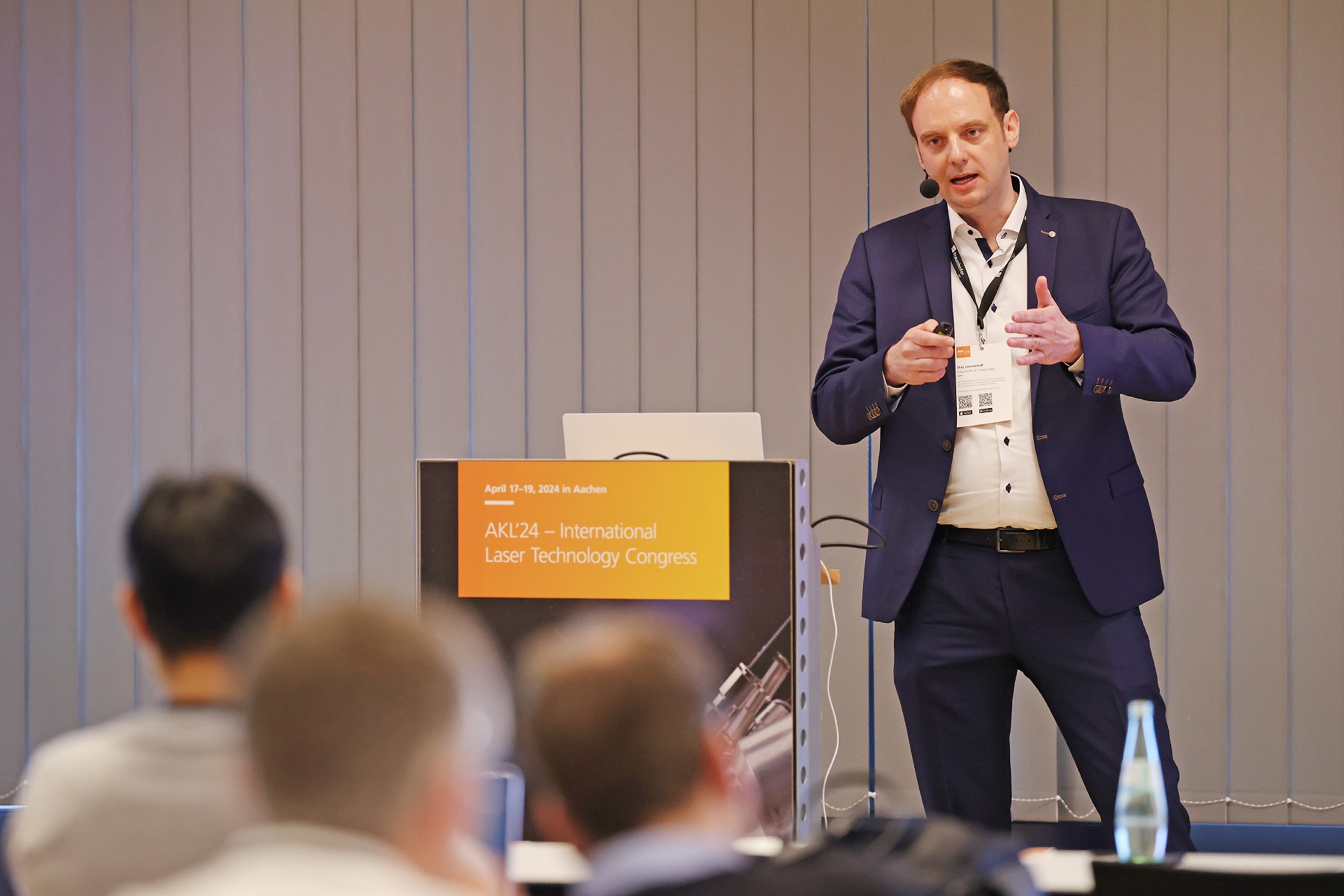
Laser-induced forward transfer technology (LIFT) can be used to transfer very thin and precise layers of materials onto substrates. Ara-Coatings GmbH & Co KG from Nordhorn uses this technology to create functional layers in electronic, optical and biomedical applications. In LIFT, physical vapor deposition (PVD) and laser technology are combined to transfer materials with specific functional properties selectively and without a vacuum. This saves considerable costs because coatings can be produced quickly, efficiently and without further pre- or post-treatment. The LIFT process can be applied to a wide range of materials with different properties in terms of stoichiometry, crystal structure and electrical conductivity, explained Ara Coatings expert Dr. Ralph Domnick. He emphasized how scalable and flexible the process is. For example, it can generate coating thicknesses of around 0.5 µm to 5 µm and ultra-fine conductor paths of just 12 µm in width. In addition, the coating speed is impressive: Despite the precision, an area of one square meter can be completely coated in just three minutes.
AKL’24 also focused on how functional layers could be selectively applied to a component in order to alter its surface properties exactly where it is required, or also how to repair worn and damaged areas. Dr. Ralph Delmdahl, Senior Product Marketing Manager at Coherent LaserSystems GmbH & Co. KG in Göttingen, dedicated his presentation to an innovative laser process for the mass production of high-temperature superconductor (HTS) tapes: Pulsed laser deposition (PLD) can deposit crystalline thin films in a precisely controlled material composition. A wide range of oxides, nitrides, carbides, sulfides, polymers and 2D materials are available for this purpose. They can be processed by PLD into micrometer-thin monolayers whose density, morphology and other parameters can be varied via the laser settings. Excimer lasers with a high energy output in the ultraviolet wavelength range are used as lasers. According to Delmdahl, HTS tapes produced using PLD are considered a game changer in applications such as magnetic nuclear fusion in TOKAMAK reactors.
Laser-based material application is not only used for coating, but also for repairs. At AKL’24, Dr. Johannes Finger from Aachen-based IIC-AM GmbH, which is part of the globally active Makino Group, provided examples of this. He emphasized the high speed of laser-based deposition of powder materials, a speed that is accompanied by efficient process control and high material utilization, but also places minimal thermal stress on the repaired components. This method is particularly suitable for applications in which high material quality and precise control of microstructures are important. Among other things, he showed multi-material components and repair inserts on impellers and turbine blades. Makino developed the process in collaboration with Fraunhofer ILT, among others.
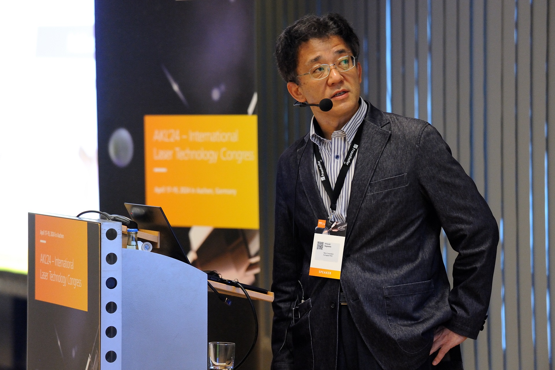
The closely related direct energy deposition (DED) process was the focus of further AKL presentations on laser-based repair processes. Hiroyuki Nagasaka demonstrated products and applications from Nikon in Japan under the title “Light as eyes and as a tool.” Precise 3D material deposition and ablation are combined with integrated, three-dimensional measurement processes for real-time quality monitoring; thus, complex components such as turbine blades can be repaired with high material utilization and produced using support structure-free 3D printing with minimized rework. Nikon relies on the precision of USP laser processes, among other things. Nagasaka used the AKL’24 to showcase the concern's next generation of DED systems.
The “Scan-Repair” approach from DMG MORI Ultrasonic Lasertec GmbH follows a similar methodology. 3D scanners measure worn or damaged components, which are clamped in a 5-axis system and run through a defined scanning process. The data obtained is compared with the CAD data of the parts in order to determine what needs to be repaired and immediately derive the appropriate repair strategy. A DED process is used, in which a 3.5 kW laser melts the metal powder flowing from nozzles in layers onto the damaged areas. A camera system records the emissions from the molten bath for quality control purposes. After the laser application, the component is processed mechanically in the hybrid process in order to produce the exact component contour and required surface quality.
The repair and reconditioning of worn and damaged components is sustainable, conserves resources and is considered an important prerequisite for entering the circular economy. Dr. Gentry Wood from Apollo-Clad Laser Cladding in Edmonton, Canada, explained the company's own laser processing technology in his presentation “LMD for the manufacture, repair and improvement of complex components.“ Originally, Apollo-Clad mainly served the oil and gas industry. However, more and more customers from the agricultural sector are now asking for repairs and ultra-hard coatings. In his AKL presentation, Wood reported on how the company achieved significantly better results for this target group by adjusting the process parameters when machining tungsten carbide in a Ni-Cr-B-Si matrix. “Although the modified alloy is not as hard, it is cheaper and the machining process is faster. The tendency to crack is also reduced,” explained Wood.
Josh Barras from the TWI Technology Center in Catcliffe (UK) made a similar point. His presentation “Applications and case studies for functional surfaces using Extreme High Speed Laser Material Deposition” highlighted the advantages of the EHLA process for repair processes. “The speed of the now widely established process offers economic advantages and makes it interesting for many applications,” he explained in his presentation.
Quantum technologies are considered an important field for the future. The European Union and Germany are striving for technological sovereignty and a leading international role. They are therefore investing heavily in research funding. The USA, China, India, the UK, and other countries are pursuing similarly ambitious goals and are also investing billions in funding. The AKL’24 “Quantum Technology & Photonics” forum saw the first successes of these investments.
Particularly in the areas of quantum computing and quantum networks, great strides are being made. Highlights included two presentations on quantum networks: one team each from Delft (NL) and New York (USA) presented “real” quantum networks - networks in which not only codes are exchanged, but also entanglement is created. Thanks to this entanglement, which Einstein once called “spooky”, the properties of the photon pairs remain so closely correlated despite spatial separation that the measurement of one photon is sufficient to know the state of the second. This effect makes it physically impossible for third parties to listen in on entangled quantum pairs.
Such a network is extremely difficult to establish because light signals cannot be stored as easily as electrical signals. However, if the signals from two partners are to be superimposed at a third node, then one signal must wait until the other arrives. Ronald Hanson‘s group at QuTech in Delft has now developed a solution for this: a storage system for single photons with nitrogen-doped diamond crystals.
Using this storage, they have successfully established a quantum connection between three cities in which entanglement was also transferred. This had already been possible before in the laboratory, but this was the first time such a connection between several cities had been demonstrated anywhere in the world. Mehdi Namazi (Chief Science Officer, Qunnect, New York) presented a similar experiment in New York, in which the group there used quantum memories with rubidium atoms.
A crucial subsystem for the experiments in Delft came from Aachen: The quantum storage uses photons of a wavelength that cannot be transmitted well in telecommunication fibers. The individual photons must, therefore, be converted between transport and storage. A team at Fraunhofer ILT has developed a quantum frequency converter for this purpose, as Fabian Geus reported. At over 40 percent, its efficiency is particularly high. By using periodically poled lithium niobate, the institute was able to increase the signal-to-noise ratio in the system by a factor of 100.
Alongside all the successes, Marc Geitz from Deutsche Telekom AG's T-Labs had a more reflective tone. He and his team in Berlin are investigating how quantum computers and quantum networks can be used for industrial applications. To this end, he has tested various approaches and different computers. His conclusion: “We are not there yet.” So far, the quantum advantage is manageable, any yet he would like to see better quantum hardware, more qubits, more connectivity.
Dr. Stefan Hengesbach, CEO of QuiX Quantum in Enschede (NL), is working on exactly that. His company develops optical quantum computers. He thinks that 100,000 to a million physical qubits are needed to be able to offer enough logical qubits. “That will take a few years,” said the former ILT employee. QuiX currently has a system with 12 qubits, although they are working internally on a 20 qubit processor. The necessary components can largely be accommodated on a semiconductor chip, and further scaling is foreseeable. The bottleneck for him is still the single photon sources. He hopes to be able to present a good solution for this at AKL’26.
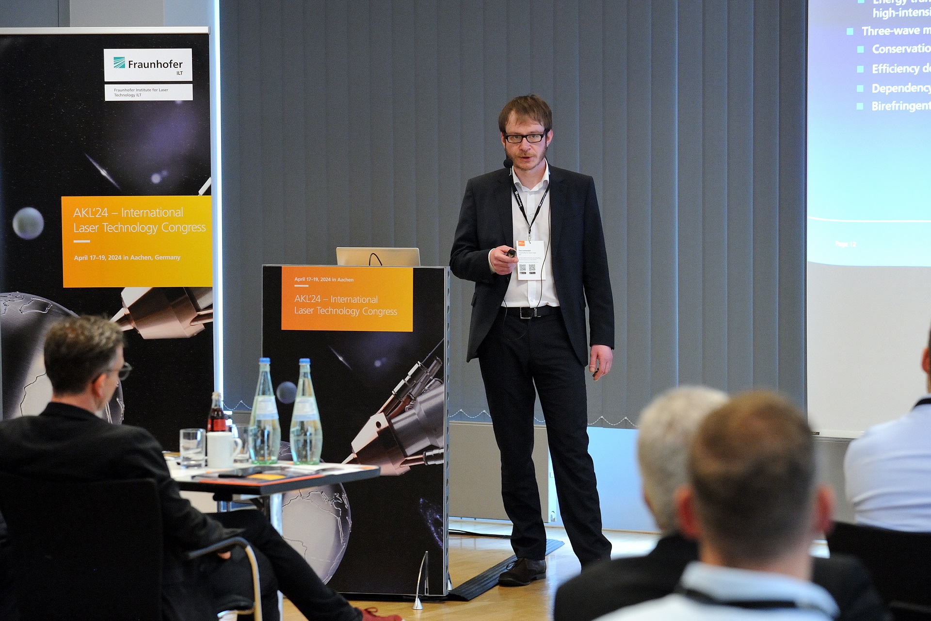
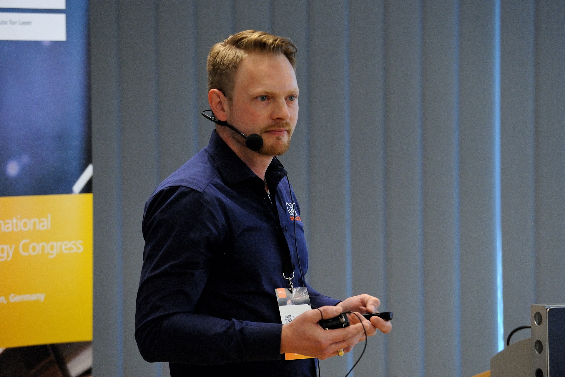
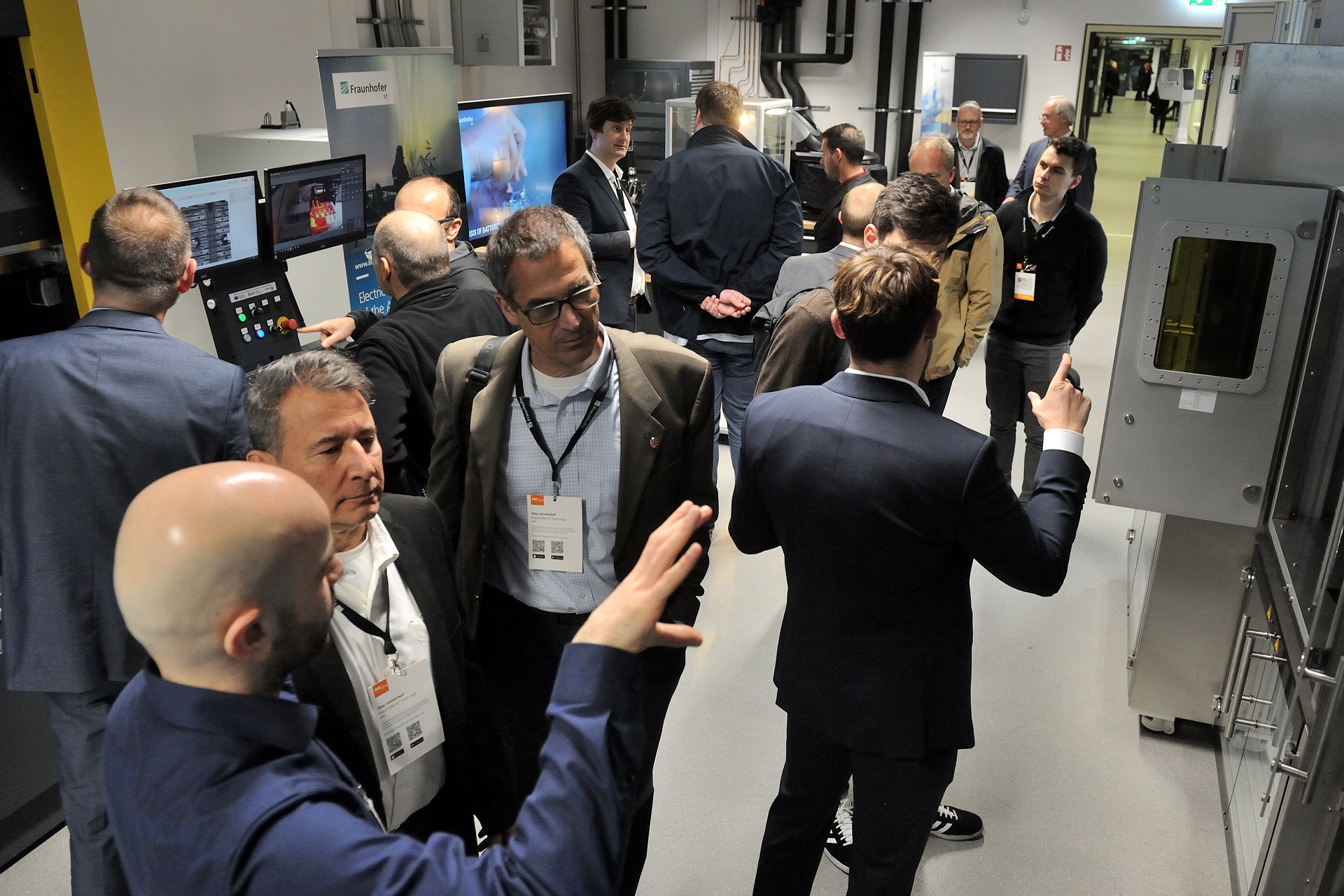
When Peter Leibinger predicted in 2013 that lasers would become a commodity, he was met with a great deal of skepticism. But his prediction has come true. Today, laser beam sources for established applications such as cutting and welding are largely standardized products that function at a high technical level. Fiber lasers are considered workhorses; their parameters are becoming increasingly similar across manufacturers. As a result, competition and cost pressure are increasing.
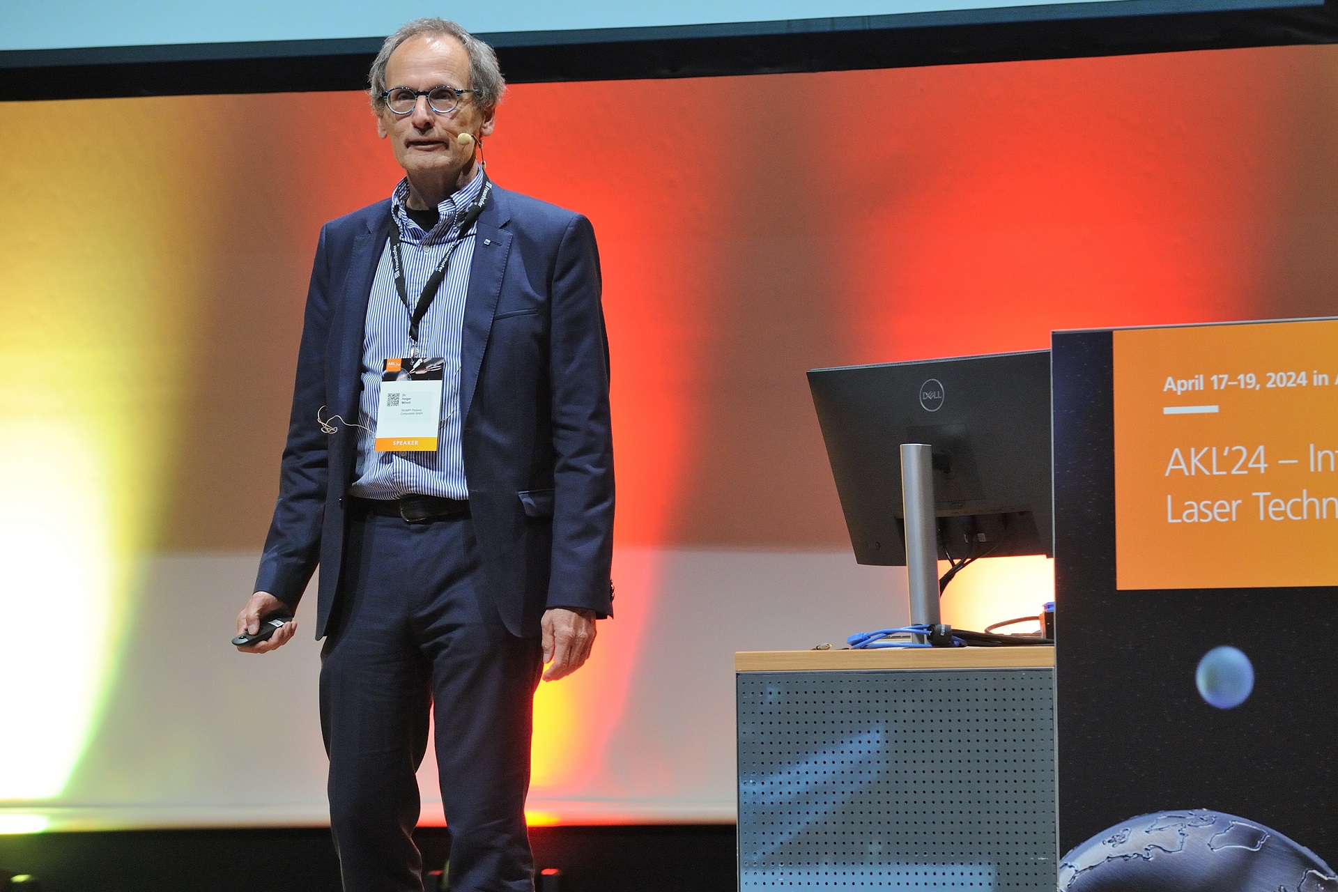
In response to this, laser manufacturers are shifting their focus: They are no longer just interested in being better than conventional solutions, but also in making their products and processes more cost-effective. A good example of this is heating with VCSELs, vertically emitting diode lasers, which have efficiency values of more than 60 percent. As Holger Mönch from TRUMPF Photonic Components reported at AKL’24, the demand for VCSELs is increasing in energy-intensive processes such as the drying of lithium battery electrodes. This is because the high energy efficiency quickly pays for itself in such multi-kW applications.
Annealing is another large-scale laser application relevant here. Display manufacturers use this type of heat treatment to convert amorphous silicon into polycrystalline silicon. Large excimer lasers have been used for this for decades. However, as Robin Rammelsberg from COHERENT in Aachen reported, the switch to solid-state lasers is currently underway. This is because they combine the same beam parameters as excimer lasers with lower operating costs, especially as the time-consuming gas exchange is no longer necessary. As laser annealing is widely used in display production, a large market is opening up here that will also attract other suppliers of solid-state lasers.
More power from the diodes, new wavelengths and more powerful short-pulse systems: This is how the other presentations at the AKL sessions on beam sources described the current trends. In particular, there have been many advances in short-pulse laser systems in recent years. Industry’s focus here is shifting from systems for the research sector towards industrial applications: TRUMPF is now offering a system with 1 kW output power for the first time, which should provide a leap in efficiency in large-scale material processing. However, the scaling to high outputs will continue. Current research into “secondary sources” – laser-based sources for X-rays, electrons and particle beams – is driving this development.
Also at AKL’24 were EKSPLA and Light Conversion, two Lithuanian suppliers that are among the global market leaders in the field of short-pulse lasers. EKSPLA supplies top addresses all over the world, including NASA, CERN, ELI, the Massachusetts Institute of Technology (MIT) and various Max Planck Institutes. Here, too, attention is shifting towards high-performance femto-, pico- and nanosecond lasers for industry. Martynas Barkauskas, CEO of Light Conversion from Vilnius, which has already delivered around 9,000 systems worldwide, also reported on new developments in frequency conversion in the ultraviolet and infrared range in his presentation.
The demand for higher efficiency and power is directed at all lasers, but diode lasers in particular. Steve Patterson, CTO of Leonardo Electronics US, dedicated his presentation to high-power diode laser modules, which the company is developing with a focus on laser-ignited inertial fusion energy (IFE). The efficiency of such diode lasers is considered a decisive factor in promoting the commercial use of climate-neutral fusion energy. According to Patterson, Leonardo has already supplied diode laser modules to several fusion research facilities and is also involved in German research projects.
The technological and economic potential of fusion power plants was also the subject of the concluding plenary lecture by Prof. Constantin Haefner. The Institute Director of Fraunhofer ILT emphasized the need for high-energy and efficient diode lasers. These are the key to providing the required laser pumping power in the megawatt range, which is essential for the continuous ignition of fusion. Haefner also described how highly dynamic the future technology is, as it pushes forward from basic into application-oriented research and development worldwide. The focus: new lasers, new optical systems and new approaches in the complex engineering of intrinsically safe, climate-neutral fusion power plants.
As challenging as the technological tasks are, the economic prospects are just as promising. If the entry into commercial IFE use is successful, a global market with enormous potential will open up for the laser industry and for suppliers of high-performance optical components. Haefner had already focused on photonic markets of the future at the Gerd Herziger Session of AKL’24: Looking ahead, he saw huge, completely untapped markets for photonics with many hundreds of billions of euros in sales potential – including quantum technologies, sustainability, secondary sources, cyberphotonics and inertial fusion.
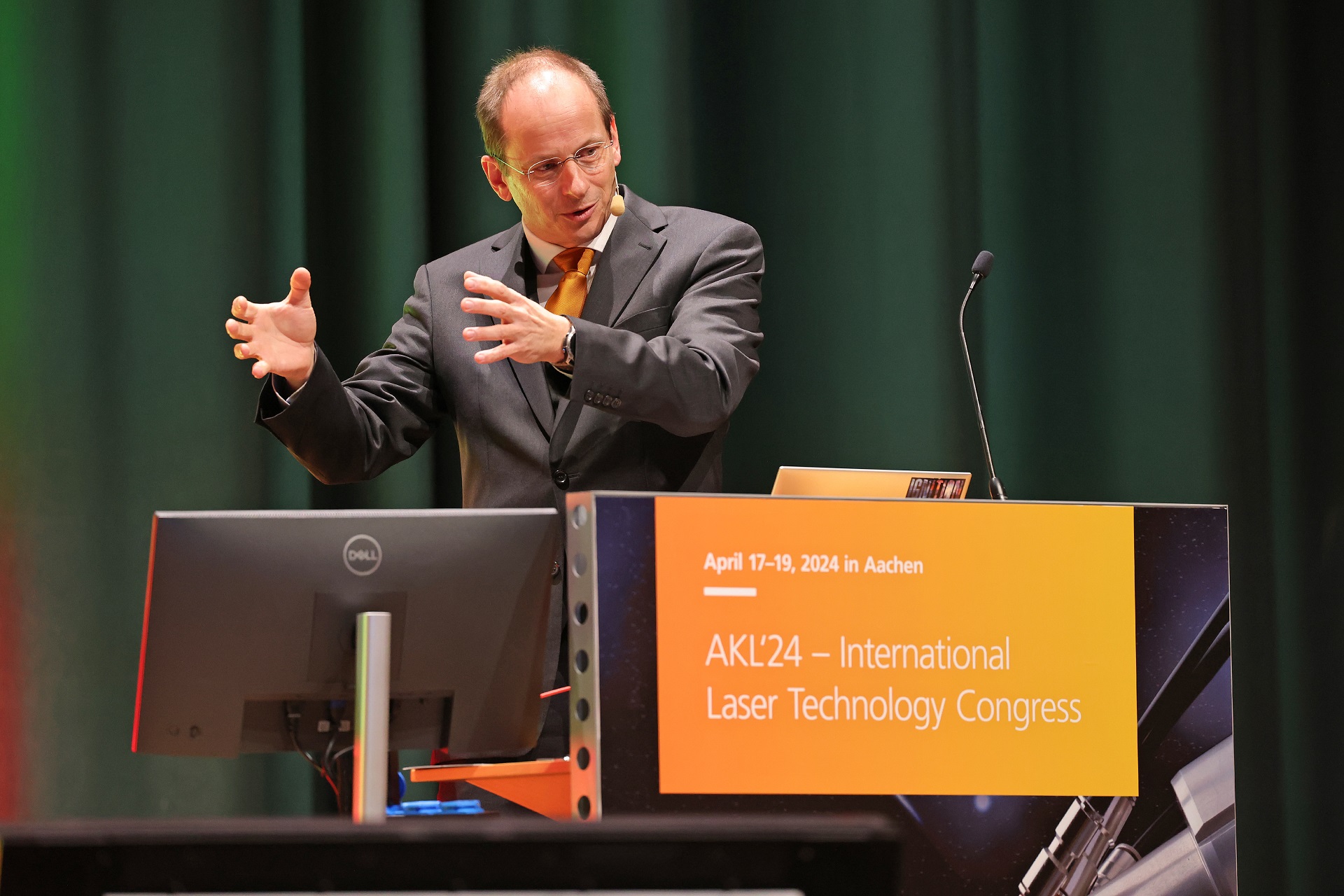
While the actual laser is the same in many systems, there are considerable differences in the optical systems, as Andrea Braglia, managing director of nLight Europe, pointed out in his presentation. The specific design of the beam profiles ensures efficiency in the application and optimally adapts the laser beam to the respective requirement profile in the process. In order to differentiate laser systems from the competition through the design of the optical systems, maximum precision and high flexibility are essential.
Accordingly, all the stops of modern optics are being pulled out for beam shaping. Stephen Kidd from PowerPhotonic in Scotland, for example, presented innovative approaches with freeform optics and phase plates as well as optical solutions for coherent beam combination. According to Prof. Carlo Holly, head of the Chair of Technology of Optical Systems TOS at RWTH Aachen University and head of the Data Science and Metrology Department at Fraunhofer ILT, the use of artificial intelligence is currently opening up new perspectives in the design of such complex optical systems.
In his presentation, Holly gave an outlook on the future of calculating optical systems: Trained with the knowledge and experience of today's optical designs, AI will work out the dimensions of any beam profile. Here, too, the focus is on individually adapting the optical system to the respective process – and in the medium term on laser-based first-time-right production, in which the optimized beam profiles play a central role.
The importance of innovative beam shaping designs for industrial laser technology was also demonstrated by the jury's decision for this year‘s Innovation Award Laser Technology, which was presented by the Arbeitskreis Lasertechnik e.V. at AKL’24: CAILABS from Rennes, France, was among the winners. The prize was awarded to their beam shaping technology for high-performance laser material processing. This so-called multi-plane light conversion (MPLC) modifies the intensity distribution of processing lasers, paving the way for higher process speeds and improved quality at the same time. Among other things, the tailored beam shaping optimizes laser welding processes for copper and aluminum because the adapted intensity distribution minimizes the formation of pores and spatter.
Traditional manufacturing processes such as laser cutting and welding were the focus of the “Cutting and Joining” session at AKL’24. Dr. Alexander Olowinsky, head of the Joining and Cutting Department at Fraunhofer ILT, describes a common thread running through the various processes presented at the congress: “The demand is not only for faster and more efficient processes as before, but now also for flexibility and documented, verifiable quality, while also having all processes fully integrated into digital process sequences”.
There are different ways to achieve this: A new laser cutting system from Automatic-Systeme Dreher GmbH from Sulz am Neckar shows how flexibility, productivity and sustainability can be significantly increased by using two laser heads and gantries. Managing Director Hasan Sarac pointed out the advantages of the innovative interaction between the gantries. It significantly improves nesting, which is the arrangement of components on the belt, and reduces material waste from 29 to just 6 percent compared to conventional punching. The system design also enables manufacturers to process smaller batch sizes without needing to retool: This shortens throughput times and maintains productivity, while belt speed remains the same.
Those who consistently exploit the potential of digitalization will sooner or later come across new business models. This is also the case at TRUMPF-Werkzeugmaschinenfabrik GmbH in Ditzingen, which presented its new remote operation concept: Laser cutting systems can be controlled and monitored remotely. According to the Global Product Manager of this solution, Benedikt Braig, this enables users to access the interconnected machines externally and to do efficient troubleshooting without the physical presence of a technician. In return, customers have to make a long-term commitment, i.e. enter into a long-term business relationship with TRUMPF. This aspect was discussed quite controversially by the participants in the session. “This system only makes sense if the company is planning a long-term cooperation with TRUMPF. At least six years was discussed,” summarized Olowinsky.
Artificial intelligence (AI) is also becoming increasingly important in the field of laser cutting. For example, the Fraunhofer ILT relies on machine learning when cutting bipolar plates for fuel cells and battery components. “So far, we have mainly used it to evaluate process signals. The next step will be AI-supported process development,” explained Dr. Frank Schneider, head of the Institute’s Cutting Group.
But it doesn't always have to be electronics: PT Photonics Tools GmbH from Berlin relies on a tactile guide wire system for its laser for welding and soldering, which precisely aligns the beam along the weld seam. This simplifies the process considerably and makes the use of complex cameras for seam detection superfluous. Thanks to the use of filler wire as a guide element, targeted bends and deformations of the wire can be used to precisely position the laser focus.
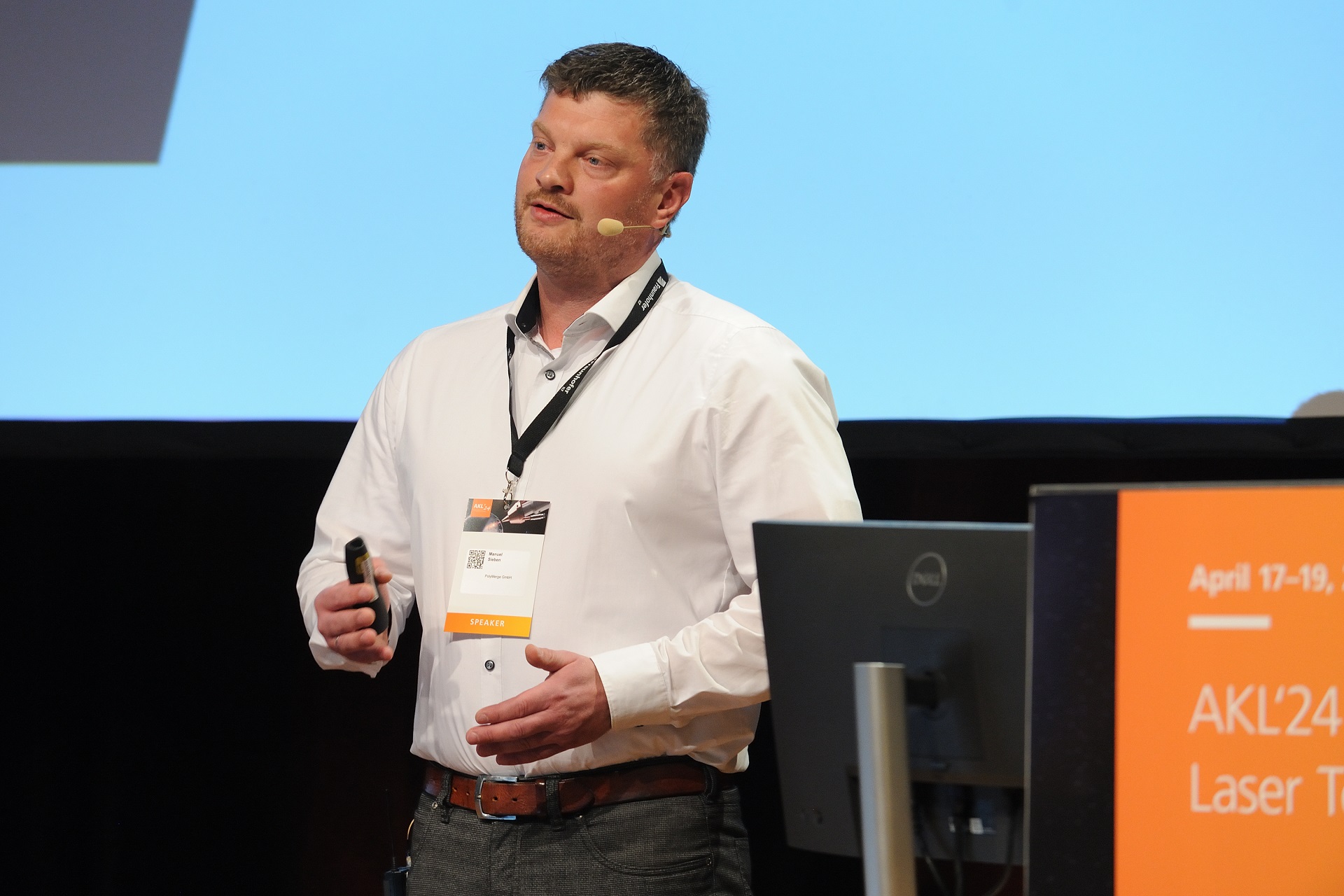
PolyMerge GmbH from Geretsried presented new approaches to plastic welding. According to Managing Director Manuel Sieben, scanner-based laser welding with a conical mirror involves the efficient joining of cylindrical components. He presented applications for laboratory use, for high quantities and for mass production, which the company realizes with an ultra-flexible, modular machine design. Combined with motorized beam expansion, spot sizes of 0.8 to 3.00 millimetres are possible. He also gave some insight into a patented infrared welding process based on additively manufactured ceramic emitters. Olowinsky: “Both technologies increase flexibility, speed and efficiency – especially in prototype construction.”
Research associate Friederike Brackmann from Fraunhofer ILT, who is developing laser processes for the textile industry in the Micro Joining research field, hinted at the future. In Aachen, she presented a laser bonding process that can be used to join conductive tracks to thermoplastic textiles without significant heat input. Laser bonding creates a strong connection by melting the plastic part of the textile through the heated copper track. The aim is to create smart textiles that light up as T-shirts or measure temperature and moisture as sensory mattress toppers. The process replaces traditional methods such as weaving or embroidering wires, which impair the flexibility of the textiles.
Another pioneering laser application was presented by Dr. Jens Gottmann, Managing Director of LightFab GmbH from Aachen. The company, which is based at the Digital Photonic Production research campus, uses ultrashort pulse (USP) lasers for selective laser etching (SLE) to produce complex, microstructured, transparent components directly from 3D CAD data. LightFab system technology is already being used for prototypes and series production in medical technology, precision mechanics and optics.
Olowinsky is thoroughly satisfied with the outcome of the session. “The high number of participants and the positive response to the presentations underline the interest in modern laser-based cutting and joining processes,” he comments. There is great potential for innovation when companies integrate established laser applications into digital process chains, combine different processes, and, above all, use AI.
AKL’24 also focused on the latest developments in additive manufacturing (AM). Advances in process control, energy consumption, sustainability and materials are evidence that this young technology is becoming mature.
Dr. Stefan Leuders from the voestalpine Additive Manufacturing Center Düsseldorf also emphasized this in his presentation “Additive Manufacturing for sustainable tooling applications.” Like other speakers, he pointed out that the manufacturing industry can use AM to increase its efficiency, contribute to environmental protection and also reduce its costs. “A tool costing ten to fifteen thousand euros can often be repaired for one to two thousand euros,” explained Leuders. At the same time, consistent repair and reuse saves many thousands of tons of CO2 and uses resources much more efficiently. He countered skeptics with the increased quality of AM parts. The integrity and performance of additively manufactured parts is constantly improving thanks to new methods of heat treatment and cooling, among other things.
Frank Rethmann from Airbus Helicopters GmbH in Donauwörth discussed the current “Status Quo and perspectives of AM for series production in the aerospace industry.” He showed how the company is systematically approaching the industrialization of additive processes and working towards the series use of additively manufactured metal and plastic components in helicopters. Qualification, systematic screening of components and assemblies that are suitable for AM and consistent automation are paving the way. At the same time, it is also important to use new materials, optimize process parameters and apply new approaches to increase productivity across the entire process chain from design to post-processing.
Andrew Bayramian presented the work of Seurat Technologies from Wilmington, Massachusetts. The high-power laser technology “Area Printing” is a scalable AM method for powder bed-based laser beam melting. A key feature of the technology is its high throughput rate, which the company achieves by using millions of laser dots simultaneously. This breaks with the traditional paradigm that high resolution comes at the expense of throughput. Seurat was able to improve both aspects in parallel by decoupling speed and resolution. The key to this is a three-stage approach in which a laser first preheats the surface to be exposed at low intensity. In the next step, pulsed high-intensity laser beams hit the heated powder, melting it in the already preheated component contour of the area in question. This vaporizes the top metal layer and presses the molten powder onto the layer below. This surface exposure leads to a considerable increase in the build-up rate. According to Bayramian, this opens up new application possibilities in industries that have hardly used 3D printing processes for metals to date. He sees good opportunities to open the door to economically competitive AM mass production.
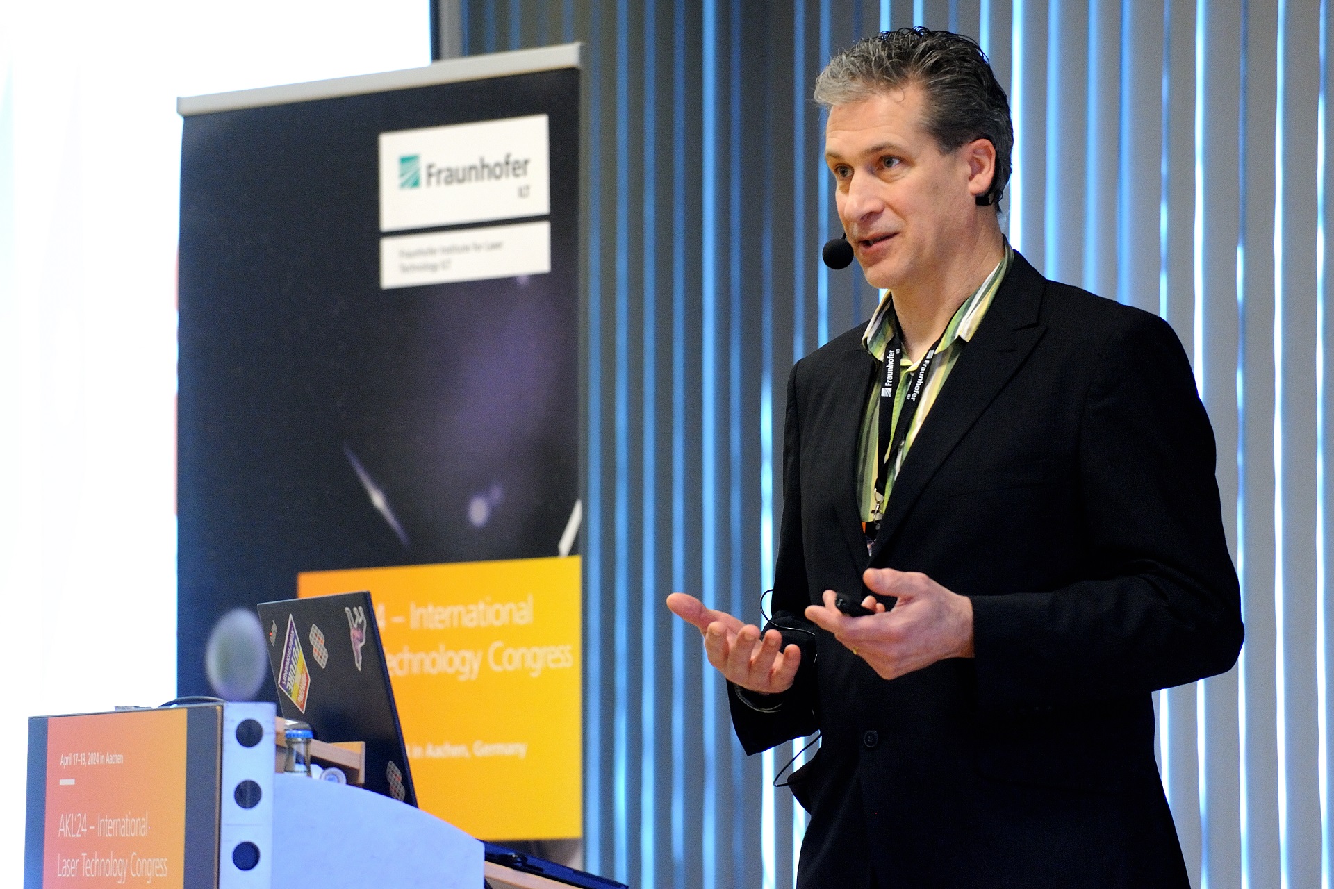
But it is not only additive processes that are making progress. In his presentation, Kaushik Budhelyia from LightFab in Aachen provided information in his presentation “New developments in selective laser etching (SLE) for photonic applications.” The SLE approach makes high-precision, subtractive 3D printing in glass bodies possible. The material to be removed is selectively exposed by a laser with micrometer precision, which makes the material more vulnerable to subsequent wet-chemical etching process than the untreated glass. It dissolves and can be rinsed out of the contour. This way, channels, cavities and other shapes of almost any shape can be created. Applications range from electronics and the automotive industry to ion traps for quantum computers or lab-on-chip solutions for medical diagnostics. Microfluidics systems produced with SLE are used for rapid tests for antibiotic resistance and for cell sorting and analysis, among other things.